- 您现在的位置:买卖IC网 > Sheet目录307 > ADE7752BARWZ-RL (Analog Devices Inc)IC ENERGY METERING 3PHASE 24SOIC
ADE7752B
HPF AND OFFSET EFFECTS
+ V OS OS + V OS × I cos ( ω t ) + I OS × V cos ( ω t ) (10)
× I
× cos ( 2 ω t )
V × I
Figure 20 shows the effect of offsets on the active power
calculation. An offset on the current channel and the voltage
channel contributes a dc component after multiplication, as
shown in Figure 20. Because this dc component is extracted by
the LPF and is used to generate the active power information
for each phase, the offsets can contribute a constant error to the
total active power calculation. The HPF in the current channels
avoids this problem easily. By removing the offset from at least
one channel, no error component can be generated at dc by the
multiplication. Error terms at cos(ωt) are removed by the LPF
and the digital-to-frequency conversion (see the Digital-to-
Frequency Conversion section).
{ V cos ( ω t ) + V OS } × { I cos ( ω t ) + I OS } =
V × I
2
+
2
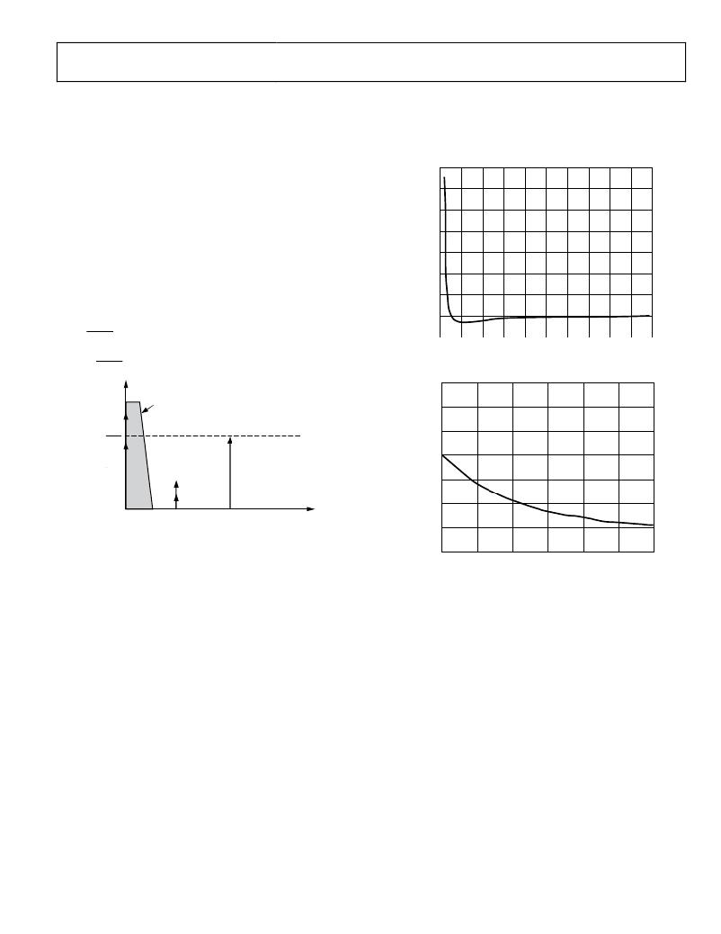
The ADE7752B is phase compensated up to 1 kHz as shown. This
ensures correct active harmonic power calculation even at low
power factors.
0.07
0.06
0.05
0.04
0.03
0.02
0.01
0
–0.01
0 100 200 300 400 500 600 700 800 900 1000
FREQUENCY (Hz)
Figure 21. Phase Error Between Channels (0 Hz to 1 kHz)
0.010
V OS × I OS
V× I
DC COMPONENT (INCLUDING ERROR TERM)
IS EXTRACTED BY THE LPF FOR REAL
POWER CALCULATION
0.008
0.006
2
0.004
I OS × V
V OS × I
0.002
0
0
ω
2 ω
FREQUENCY (RAD/sec)
–0.002
Figure 20. Effect of Channel Offset on the Active Power Calculation
The HPF in the current channels has an associated phase response
that is compensated for on-chip. Figure 21 and Figure 22 show the
phase error between channels with the compensation network.
Rev. 0 | Page 17 of 24
–0.004
40 45 50 55 60 65
FREQUENCY (Hz)
Figure 22. Phase Error Between Channels (40 Hz to 70 Hz)
70
发布紧急采购,3分钟左右您将得到回复。
相关PDF资料
ADE7755ARSZ
IC ENERGY METERING 1PHASE 24SSOP
ADE7757ARNZRL
IC ENERGY METERING 1PHASE 16SOIC
ADE7758ARWZRL
IC ENERGY METERING 3PHASE 24SOIC
ADE7761AARSZ-RL
IC ENERGY METERING 1PHASE 20SSOP
ADE7761BARSZ-RL
IC ENERGY METERING 1PHASE 20SSOP
ADE7768ARZ-RL
IC ENERGY METERING 1PHASE 16SOIC
ADE7769ARZ-RL
IC ENERGY METERING 1PHASE 16SOIC
ADM8843ACPZ-REEL7
IC LED DRVR WHITE BCKLGT 16LFCSP
相关代理商/技术参数
ADE7753
制造商:AD 制造商全称:Analog Devices 功能描述:Active and Apparent Energy Metering IC with di/dt sensor interface
ADE7753_10
制造商:AD 制造商全称:Analog Devices 功能描述:Single-Phase Multifunction Metering IC with di/dt Sensor Interface
ADE7753ARS
制造商:Analog Devices 功能描述:Single Phase Multifunction Metering IC 20-Pin SSOP 制造商:Rochester Electronics LLC 功能描述:- Bulk 制造商:Analog Devices 功能描述:IC SEMICONDUTOR ((NS))
ADE7753ARSRL
制造商:Analog Devices 功能描述:Single Phase Multifunction Metering IC 20-Pin SSOP T/R 制造商:Rochester Electronics LLC 功能描述:- Bulk
ADE7753ARSZ
功能描述:IC ENERGY METERING 1PHASE 20SSOP RoHS:是 类别:集成电路 (IC) >> PMIC - 能量测量 系列:- 产品培训模块:Lead (SnPb) Finish for COTS
Obsolescence Mitigation Program 标准包装:2,500 系列:*
ADE7753ARSZ
制造商:Analog Devices 功能描述:ENERGY METERING IC
ADE7753ARSZ
制造商:Analog Devices 功能描述:IC MULTIFUNCTION METER
ADE7753ARSZRL
功能描述:IC ENERGY METERING 1PHASE 20SSOP RoHS:是 类别:集成电路 (IC) >> PMIC - 能量测量 系列:- 产品培训模块:Lead (SnPb) Finish for COTS
Obsolescence Mitigation Program 标准包装:2,500 系列:*
